NaNet overview
NaNet is a FPGA-based PCIe Network Interface Card (NIC) design with Remote Direct Memory Access (RDMA) and GPUDirect P2P/RDMA capabilities featuring a configurable and extensible set of network channels.
The design supports both standard and custom channels:
- GbE (1000BASE-T)
- 10GbE (10Base-KR)
- 40GbE
- APElink (custom 34 Gbps link dedicated to HPC systems)
- KM3link (deterministic latency 2.5Gbps link used in the KM3Net-IT experiment data acquisition system)
The RDMA feature combined with of a transport protocol layer offload module and a data stream processing stage makes NaNet a low-latency NIC suitable for real-time processing of data streams.
NaNet GPUDirect capability enables the connected processing system to exploit the high computing performances of modern GPUs on real-time applications.
Since January 2015 NaNet is an ![]() INFN Scientific Committee 5 funded experiment.
INFN Scientific Committee 5 funded experiment.
Here you can find a list of publications and talks about the project.
NaNet Architecture
NaNet design is partitioned into 4 main modules: Router, Network Interface, PCIe Core, and I/O Interface (see ig.1).

- The Router module supports a configurable number of ports implementing a full crossbar switch responsible for data routing and dispatch. Number and bit-width of the switch ports and the routing algorithm can all be defined by the user to automatically achieve a desired configuration. The Router block dynamically interconnects the ports and comprises a fully connected switch, plus routing and arbitration blocks managing multiple data flows @2.8 GB/s.
- The Network Interface block acts on the trasmitting side by gathering data incoming from the PCIe port and forwarding them to the Router destination ports; on the receiving side it provides support for RDMA in communications involving both the host and the GPU (via a dedicated GPU I/O Accelerator module). A NIOS-II microcontroller handles configuration and runtime operations.
- The PCIe Core module is built upon a powerful commercial core from PLDA that sports a simplified but efficient backend interface and multiple DMA engines.
- The I/O Interface module is the discriminating component among the cards in the NaNet family. It is each time re-designed in order to satisfy the requirements of the readout system data transmission protocol optimizing the data movement process for the different experiments. The I/O Interface module performs a 4-stages processing on the data stream: following the OSI Model, the Physical Link Coding stage implements, as the name suggests, the channel physical layer (e.g. 1000BASE-T, 10GBASE-R, etc.) the Protocol Manager one handles data/network/transport layers (e.g. Time Division Multiplexing or UDP), depending on the kind of channel; the Data Processing stage implements application-dependent reshuffling on data streams (e.g. performing de/compression) while the APEnet Protocol Encoder performs protocol adaptation, encapsulating inbound payload data into the APElink packet protocol — used in the inner NaNet logic — and decapsulating outbound APElink packets before re-encapsulating their payload into the output channel transport protocol (e.g. UDP).
This general architecture has been specialized into several configurations to match the requirements of different experimental setups:
- NaNet-1 featuring a PCIe Gen2 x8 host interface plus a GbE one, three optional 34 Gbps APElink channels and is implemented on the Altera Stratix IV FPGA Development Kit.
- NaNet3 implemented on the Terasic DE5-NET Stratix V FPGA development board sporting four SFP+ cages. It supports four 2.5~Gbps deterministic latency optical KM3link channels and a PCIe Gen2 x8 host interface.
- NaNet-10 featuring four 10GbE SFP+ ports along with a PCIe x8 Gen2/Gen3 host interface and also implemented on the Terasic DE5-NET board.
- NaNet-40 featuring two 40GbE QSFP+ ports along with a PCIe x8 Gen3 host interface, implemented on the Bittware S5-PCIe-HQ board (with Altera Stratix V)
The board is able to manage either 34 Gbps APElink channel or 1/10/40 GbE interfaces and exploit the GPUDirect P2P capabilities of nVIDIA Fermi/Kepler/Maxwell/Pascal GPUs equipping a hosting PC to directly inject into their memory an UDP input data stream from the detector front-end, with rates compatible with the low latency real-time requirements of the trigger system.
In order to render harmless the unavoidable OS jitter effects that usually hinder system response time stability, the main design rule is to partition the system so that the hosting PC CPU can be offloaded from any data communication or computing task, leaving to it only system configuration and GPU kernel launch tasks. Within NaNet, this meant that data communication tasks were entirely offloaded to a dedicated IP/UDP protocol-handling block directly communicating with the P2P logic: this allows a direct (no data coalescing or staging is performed) data transfer with low and predictable latency on the GbE link → GPU data path.
Incoming data streams are processed by a Physical Link Coding block feeding the Data Protocol Manager that in turn extracts the payload data. These payload data are encapsulated by the NaNet Controller and sent to the APEnet+ Network Interface.
The Distributed Network Processor (DNP)[1] is the APEnet+ core logic, acting as an off-loading engine for the computing node in performing inter-node communications. The DNP provides hardware support for the Remote Direct Memory Access (RDMA) protocol guaranteeing low-latency data transfers. Moreover, APEnet+ is also able to directly access the Fermi/Kepler/Pascal-class NVIDIA GPUs memory (provided that both devices share the same upstream PCIe root complex) leveraging their peer-to-peer capabilites. This is a first-of-its-kind feature for a non-NVIDIA device (GPUDirect RDMA being its commercial name), allowing unstaged off-board GPU-to-GPU transfers with unprecedented low latency.
On fig. 2 we show a recap of the used FPGA logic resources as measured by the synthesis software.
NaNet Architecture and Data Flow
- APEnet+ Firmware Customization.
- UDP offload collects data coming from the Altera Triple-Speed Ethernet Megacore (TSE MAC) and extracts UDP packets payload, providing a 32-bit wide channel achieving 6.4~Gbps, discharging the Nios II from the data protocol management.
- NaNet Controller (CTRL) encapsulates the UDP payload in a newly forged APEnet+ packet, sending it to the RX Network Interface logic.
- RX DMA CTRL manages CPU/GPU memory write process, providing hw support for the Remote Direct Memory Access (RDMA) protocol.
- Nios II handles all the details pertaining to buffers registered by the application to implement a zero-copy approach of the RDMA protocol (OUT of the data stream).
- EQ DMA CTRL generates a DMA write transfer to communicate the completion of the CPU/GPU memory write process.
- A Performance Counter is used to analyze the latency of the GbE data flow inside the NIC.
Software Stack
Software components for NaNet operation are needed both on the x86 host and on the Nios II FPGA-embedded μcontroller. On the x86 host, a GNU/Linux kernel driver and an application library are present.
The application library provides an API mainly for open/close device operations, registration (i.e. allocation, pinning and returning of virtual addresses of buffers to the application) and deregistration of circular lists of persistent receiving buffers (CLOPs) in GPU and/or host memory and signalling of receive events on these registered buffers to the application (e.g. to invoke a GPU kernel to process data just received in GPU memory, see fig. 5).
On the μcontroller, a single process application is in charge of device configuration, generation of the destination virtual address inside the CLOP for incoming packets payload and virtual to physical memory address translation performed before the PCIe DMA transaction to the destination buffer takes place.
Figure 2. An overview of NaNet resource consumption.
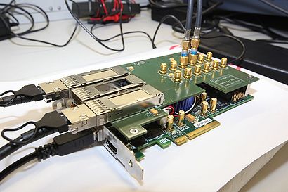
Figure 3. NaNet-1 implemented on an Altera Stratix IV coupled with a custom mezzanine card sporting 3 APE link channels.
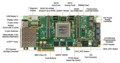
Figure 4. NaNet-10 implemented on an Altera Stratix V and featuring four 10GbE SFP+ ports.


NaNet-1
This version of the NIC features GPUDirect RDMA over 1 GbE and optionally 3 APElink channels. The design employs SGMII standard interface to connect the MAC to the PHY including Management Data I/O (MDIO); the MAC is a single module in FIFO mode for both the receive and the transmit sides (2048x32 bits). The logic resources consumption is shown in fig. 2.
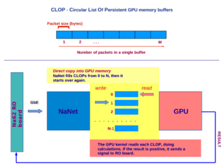
Figure 5. CLOPs scheme and their implementation in the NA62-NaNet-GPU work flow.
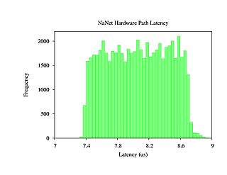
Figure 6. Distribution plot over 60000 samples of a NaNet trasversal time.

Figure 7. TEL62 to NaNet communication latency measurements performed with an oscilloscope.


NIC packets traversal latency
In order to characterize the host+NIC system, a “system loopback” configuration was used: connecting one GbE interface of the hosting PC to the NaNet, it was possible able to generate and receive a UDP stream in a single host process, measuring latency as the difference of host processor Time Stamp Counter register at send and receive time of the same UDP packet.
Latency inside the NIC was measured adding 4 cycles counters at different stages of packet processing; their values are stored in a profiling packet footer with a resolution of 4 ns; for a standard 1472 bytes UDP packet, traversal time ranges between 7.3 us and 8.6 us from input of NaNet CTRL to the completion signal of the DMA transaction on the PCIe bus (fig. 6).
For the same packet size, saturation of the GbE channel is achieved, with 119.7 MB of sustained bandwidth.
For scheduled improvements on the NaNet design see NaNet-10.
Preliminary tests for integration in a working environment
Tests for the integration in the NA62 experimental setup have been performed with the NaNet-1 board connecting a TEL62 to NaNet Gbe port and sending some Monte Carlo-generated events.
An example of latency measurements performed with an oscilloscope is shown in fig. 7: a bunch of 32 UDP packets is sent from TEL62 (red signal), thereby 4 PCIe completions (yellow signal) pinpoint the end of the DMA write transactions towards the GPU memory buffers, each sized 8 times the udp packet payload size.
NaNet-10
This version of our NIC is implemented on the Terasic DE5-net board equipped with an Altera Stratix V FPGA and featuring four 10GbE SFP+ ports and a PCIe Gen2 x8 connector (see fig. 3). The network adapter offers hardware support for either direct CPU/GPU memory access and the offloading engine managing the network stack protocol.
Data transmission system
Following the design guidelines for the NaNet I/O interface described in NaNet Architecture the Physical Link Coding is implemented by two Altera IPs, the 10GBASE-R PHY and the 10 Gbps MAC. The 10GBASE-R PHY IP delivers serialized data to an optical module that drives optical fiber at a line rate of 10.3125 Gbps. PCS and PMA are implemented as hard IP blocks in Stratix V devices, using dedicated FPGA resources. The 10 Gbps MAC supports 10 Mbps, 100 Mbps, 1 Gbps, 10 Gbps operating modes with Avalon-Streaming up to 64-bit wide client interface running at 156.25 MHz and MII/GMII/SDR XGMII on the network side.
We developed a custom 10 Gbps UDP/IP Core as a Protocol Manager of the I/O interface, providing full UDP, IPv4 and ARP protocols. It is derived and adapted from the FPGA- proven 1 Gbps UDP/IP open core[2] and provides an AXI-based 64-bit data interface at an operating frequency of 156.25 MHz. Several registers are exposed for UDP header settings (e.g. source/destination port and destination IP address) both in the transmit and receive side.
IP and MAC address are also fully customizable. The core offers ARP level functionalities, with a 256-entries cache for IP-to-MAC address translation. Underlying ARP communication is automatic when first packet transfer occurs and sender and receiver mutually exchange informations about their own IP and MAC addresses.
There is no data buffering internally, allowing zero latency between the Data Processing block and the Physical layer. For this reason packet segmentation and reassembly are not supported.
The Multi-Stream and Decompressor hardware components apply application-dependent modifications to accelerate the GPU computing task. Multi-Stream module analyses the received data stream and separates the packets according to the UDP destination port. A Decompressor stage was added in the I/O interface to reformat events data in a GPU-friendly fashion on the fly.
The NaNet Transmission Control Logic (NaNet TCL) encapsulates the received streams into the APEnet Protocol allowing for reuse of the overall APEnet+ architecture. Several parameters are used to configure the NaNet TCL ( i.e. packet size, port id, target device) and whatever is needed to fulfill the key task of virtual address generation for the APEnet packets. All the information for the virtual memory management is provided by the on-board micro-controller (base address, buffer size, number of available buffers).
Performance Analysis
NaNet-10 performances are assessed on a SuperMicro Server. The setup comprises a X9DRG-HF dual socket motherboard — Intel C602 Patsburg chipset — populated with Intel Xeon E5-2630 @2.60 GHz CPUs ( i.e. Ivy Bridge micro-architecture), 64 GB of DDR3 memory and a Kepler-class NVIDIA K40m GPU.
Measurements are performed in “loop-back” configuration closing 2 out of 4 available ports on the Terasic DE5-net board. The outgoing packet payload is generated via a custom hardware module directly feeding the UDP TX. Packet size, number of transmitted packets, delay between packets and UDP protocol destination port are configured setting several NaNet-10 registers. First we measure the time-of-flight from UDP TX to UDP RX exploiting the SignalTap II Logic Analyzer tool of the Altera Quartus II suite: this is 64 clock cycles @156.25 MHz (409.6 ns).
The receiving hardware path traversal latency is profiled via cycle counter values recorded at different stages during packet processing. The values are patched into the completion payload and stored in the event queue. The adoption of a data transmission custom hardware module ensures that results are not affected by external latency sources ( i.e. DMA memory reading process). The custom module is always ready to send data exploiting the entire link capability mimicking the detector readout system “worst-case”.
A comparison between NaNet-10 and NaNet-1 latency results in the range of interest is shown in fig. 8. The NaNet-10 NIC experiences sub-microsecond hardware latency moving data to the GPU/CPU memory for buffer sizes up to ∼ 1kByte. Focusing on bandwidth, the maximum capability of the data transmission system, 10 Gbps, is already reached for a ∼ 1kByte buffer size (fig. 9).
Finally, we notice that performance of moving data from the I/O interface of the NIC to target device memory are the same for both the CPU and the GPU.
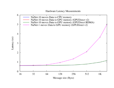
Figure 8. A comparison between NaNet-10 and NaNet-1 hardware latency.
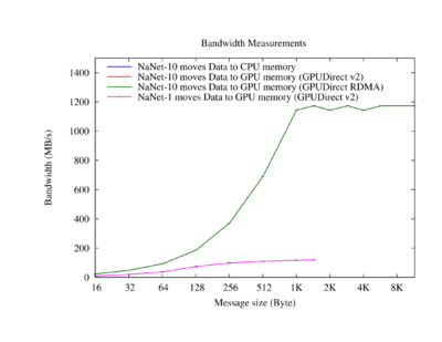
Figure 9. A comparison between NaNet-10 and NaNet-1 bandwidth.


A physics case: the Low Level trigger in NA62 Experiment's RICH Detector
NaNet is currently being used in a pilot project within the CERN NA62 experiment aiming at investigating GPUs usage in the central Level 0 trigger processor (L0TP) [3]. This is a synchronous real-time system implemented in hardware through FPGAs on the readout boards with a time budget for trigger decision of 1 ms.
The GPU-RICH processing stage is positioned between the RICH readout and the L0 Trigger Processor (L0TP) with the task of computing in real-time physics-related primitives (i.e. centers and radii of Čerenkov ring patterns on the photomultipliers arrays), in order to improve the low level trigger discrimination capability. Data from the detector photomultipliers (PMTs) are collected by four readout boards (TEL62) sending primitives to NaNet-10 as UDP datagram streams over two GbE channels (for each board, see fig. 10) connected to a GbE/10GbE switch. Packets are then routed on a 10GbE channel towards one of the NaNet-10 ports.
A processing stage on the onboard FPGA decompresses and coalesces the events fragments scattered among the several UDP streams; zero-copy DMAs towards the GPU memory are then instantiated to transmit the reconstructed events. Events are gathered and arranged in the GPU memory as a Circular List Of Persistent buffers (CLOP), according to a configurable time window which must be shorter than the total processing time to avert the overwriting of the buffers before they are consumed by the pattern recognition CUDA kernel.
A system like this, obtained retrofitting the RICH detector with a processing system capable of exploiting different kind of computing units, can be regarded as an heterogeneous “smart detector”.
Results from NA62 RUN 2017
The NaNet based system is installed close to the RICH readout rack in the NA62 experimental hall. After preliminary tests performed with NaNet-1 and a Kepler class GPU (nVIDIA K20c) in 2013-2015, it was updated to NaNet-10 in 2016 and then further improved with a Pascal class GPU (nVIDIA P100) during the NA62 2017 Run.
The test-bed is made up of a HP2920 switch, a NaNet-10 PCIe board plugged into a server made of X9DRG-QF dual-socket mother- board populated with Intel Xeon E5-2620 @2.00 GHz CPUs (i.e. Ivy Bridge architecture), 32 GB of DDR3 RAM, and a NVIDIA Pascal P100 GPU.
Latencies of the stages corresponding to GPU processing (event indexing and ring reconstruction) and sending UDP packets with the results to the L0TP are shown in fig. 11. Those are data regarding a single burst at beam intensity ∼ 19 × 1011 pps and with a gathering time for NaNet-10 of 250 μs (dashed line on plot).
The overall time is always well below the time budget limit, pointing it out as an ideal working point. Being the quality of the ring reconstruction similar to the offline and the time budget below the maximum latency allowed by the system, we conclude that the GPU trigger system implemented can be used in the future runs to design more selective and efficient trigger conditions.
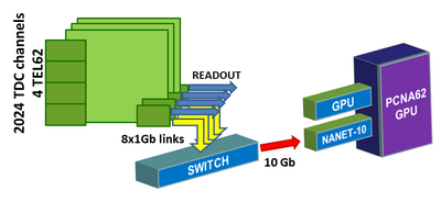
Figure 10. GPU-RICH readout system.
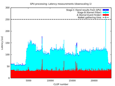
Figure 11. GPU system heterogeneous processing pipeline latency. The red area represents the latency of event indexing in the CLOP buffer (almost constant), the cyan area shows the ring reconstruction kernel latency and the blue is the sending stage.


NaNet3

To be complete, an overview of the NaNet board family must mention the undergoing development of the NaNet3 board for the KM3 HEP experiment[4]. In KM3 the board is tasked with delivering global clock and synchronization signals to the underwater electronic system and receiving photomultipliers data via optical cables. The design employs Altera Deterministic Latency Transceivers with an 8B10B encoding scheme as Physical Link Coding and Time Division MultiPlexing (TDMP) data transmission protocol. Current implementation is being developed on the Altera Stratix V development board with a Terasic SFP-HSMC daughtercard plugged on top and sporting 4 transceiver-based SFP ports.
Further enhancements
NaNet-40
To enable 40 Gb Ethernet with UDP/IP protocol hardware offload we developed this new member of the NaNet family, based on a Bittware S5-PCIe-HQ board with Altera Stratix V. It is equipped with 2 QSFP+ ports and a PCIe X8 Grn3 connector.
NaNet Public Documentation
References
- ↑ A. Biagioni, F. Lo Cicero, A. Lonardo, P.S. Paolucci, M. Perra, D. Rossetti, C. Sidore, F. Simula, L. Tosoratto and P. Vicini - The Distributed Network Processor: a novel off-chip and on-chip interconnection network architecture, March 2012. (http://arxiv.org/abs/1203.1536).
- ↑ 1g eth udp/ip stack (https://opencores.org/project/udp_ip_stack).
- ↑ G. Lamanna, G. Collazuol, Marco Sozzi - GPUs for fast triggering and pattern matching at the CERN experiment NA62, Nuclear Science Symposium Conference Record, 2009
- ↑ M. Ageron e al., Technical Design Report for a Deep-Sea Research Infrastructure in the Mediterranean Sea Incorporating a Very Large Volume Neutrino Telescope, Tech. Rep. ISBN 978-90-6488-033-9.