NaNet overview
Contents
Introduction
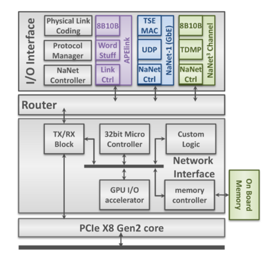
NaNet is a modular design of a low-latency NIC dedicated to real-time GPU-based systems and supporting a number of different physical links; its design baseline comes from the APEnet+ PCIe Gen 2 x8 3D NIC.
The board is able to manage either 34 Gbps APElink channel or 1/10 GbE interfaces and exploit the GPUDirect P2P capabilities of NVIDIA Fermi/Kepler GPUs equipping a hosting PC to directly inject into their memory an UDP input data stream from the detector front-end, with rates compatible with the low latency real-time requirements of the trigger system.
In order to render harmless the unavoidable OS jitter effects that usually hinder system response time stability, the main design rule is to partition the system so that the hosting PC CPU can be offloaded from any data communication or computing task, leaving to it only system configuration and GPU kernel launch tasks. Within NaNet, this meant that data communication tasks were entirely offloaded to a dedicated UDP protocol-handling block directly communicating with the P2P logic: this allows a direct (no data coalescing or staging is performed) data transfer with low and predictable latency on the GbE link → GPU data path.
The UDP OFFLOAD block comes from an open core module [1] built for a Stratix II 2SGX90 development board. Focus of that design is the unburdening of the Nios II soft-core microprocessor onboard the Stratix II from UDP packet management duties by a module that collects data coming from the Avalon Streaming Interface (Avalon-ST) of the Altera Triple-Speed Ethernet Megacore (TSE MAC) and redirects UDP packets along a hardware processing data path. The Nios II subsystem executes the InterNiche TCP/IP stack to setup and tear down UDP packet streams which are processed in hardware at the maximum data rate achievable over the GbE network.
Bringing the open core into the NaNet design required some modifications, first of all the hardware code was upgraded to work on the Stratix IV FPGA family; this upgrade made available the improved performances of an FPGA which is two technology steps ahead in respect to the Stratix II.
The synthesis performed on a Stratix IV achieves the target frequency of 200 MHz (in the current APEnet+ implementation, the Nios II subsystem operates at the same frequency). Current NaNet implementation provides a single 32-bits wide channel; it achieves 6.4 Gbps at the present operating frequency, 6 times greater than what is required for a GbE channel. Data coming from the single channel of the modified UDP OFFLOAD are collected by the NaNet CTRL. NaNet CTRL is a hardware module in charge of managing the GbE flow by encapsulating packets in the typical APEnet+ protocol (Header, Payload, Footer).
Incoming data streams are processed by a Physical Link Coding block feeding the Data Protocol Manager that in turn extracts the payload data. These payload data are encapsulated by the NaNet Controller and sent to the APEnet+ Network Interface.
The Distributed Network Processor (DNP) is the APEnet+ core logic, acting as an off-loading engine for the computing node in performing inter-node communications. The DNP provides hardware support for the Remote Direct Memory Access (RDMA) protocol guaran- teeing low-latency data transfers. Moreover, APEnet+ is also able to directly access the Fermi- and Kepler-class NVIDIA GPUs memory (provided that both devices share the same upstream PCIe root complex) leveraging their peer-to-peer capabilites. This is a first-of-its-kind feature for a non-NVIDIA device (GPUDirect RDMA being its commercial name), allowing unstaged off-board GPU-to-GPU transfers with unprecedented low latency.
NaNet Architecture and Data Flow.
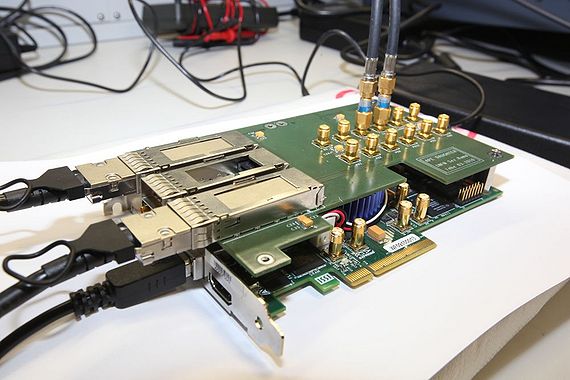
NaNet-1 implemented on an Altera Stratix IV coupled with a custom mezzanine card sporting 3 APE link channels.


NaNet Architecture and Data Flow
- APEnet+ Firmware Customization.
- UDP offload collects data coming from the Altera Triple-Speed Ethernet Megacore (TSE MAC) and redirects UDP packets into
an hardware processing data path.
- NaNet Controller encapsulates the UDP payload in a newly forged APEnet+ packet and send it to the RX Network Interface logic.
- RX DMA CTRL manages CPU/GPU memory write process, providing hw support for the Remote Direct Memory Access (RDMA) protocol.
- Nios II handles all the details pertaining to buffers registered by the application to implement a zero-copy approach of the RDMA protocol (OUT of the data stream).
- EQ DMA CTRL generates a DMA write transfer to communicate the completion of the CPU/GPU memory write process.
- A Performance Counter is used to analyze the latency of the GbE data flow inside the NIC.