NaNet overview
Contents
Introduction
NaNet is a modular design of a low-latency NIC dedicated to real-time GPU-based systems and supporting a number of different physical links; its design baseline comes from the APEnet+ PCIe Gen 2 x8 3D NIC.
The board is able to manage either 34 Gbps APElink channel or 1/10 GbE interfaces and exploit the GPUDirect P2P capabilities of NVIDIA Fermi/Kepler GPUs equipping a hosting PC to directly inject into their memory an UDP input data stream from the detector front-end, with rates compatible with the low latency real-time requirements of the trigger system.
In order to render harmless the unavoidable OS jitter effects that usually hinder system response time stability, the main design rule is to partition the system so that the hosting PC CPU can be offloaded from any data communication or computing task, leaving to it only system configuration and GPU kernel launch tasks. Within NaNet, this meant that data communication tasks were entirely offloaded to a dedicated UDP protocol-handling block directly communicating with the P2P logic: this allows a direct (no data coalescing or staging is performed) data transfer with low and predictable latency on the GbE link → GPU data path.
The UDP OFFLOAD block comes from an open core module [1] built for a Stratix II 2SGX90 development board. Focus of that design is the unburdening of the Nios II soft-core microprocessor onboard the Stratix II from UDP packet management duties by a module that collects data coming from the Avalon Streaming Interface (Avalon-ST) of the Altera Triple-Speed Ethernet Megacore (TSE MAC) and redirects UDP packets along a hardware processing data path. The Nios II subsystem executes the InterNiche TCP/IP stack to setup and tear down UDP packet streams which are processed in hardware at the maximum data rate achievable over the GbE network.
Bringing the open core into the NaNet design required some modifications, first of all the hardware code was upgraded to work on the Stratix IV FPGA family; this upgrade made available the improved performances of an FPGA which is two technology steps ahead in respect to the Stratix II.
The synthesis performed on a Stratix IV achieves the target frequency of 200 MHz (in the current APEnet+ implementation, the Nios II subsystem operates at the same frequency). Current NaNet implementation provides a single 32-bits wide channel; it achieves 6.4 Gbps at the present operating frequency, 6 times greater than what is required for a GbE channel. Data coming from the single channel of the modified UDP OFFLOAD are collected by the NaNet CTRL. NaNet CTRL is a hardware module in charge of managing the GbE flow by encapsulating packets in the typical APEnet+ protocol (header, footer and a payload whose maximum size is 4096 bytes).
Incoming data streams are processed by a Physical Link Coding block feeding the Data Protocol Manager that in turn extracts the payload data. These payload data are encapsulated by the NaNet Controller and sent to the APEnet+ Network Interface.
The Distributed Network Processor (DNP) is the APEnet+ core logic, acting as an off-loading engine for the computing node in performing inter-node communications. The DNP provides hardware support for the Remote Direct Memory Access (RDMA) protocol guaranteeing low-latency data transfers. Moreover, APEnet+ is also able to directly access the Fermi- and Kepler-class NVIDIA GPUs memory (provided that both devices share the same upstream PCIe root complex) leveraging their peer-to-peer capabilites. This is a first-of-its-kind feature for a non-NVIDIA device (GPUDirect RDMA being its commercial name), allowing unstaged off-board GPU-to-GPU transfers with unprecedented low latency.
NaNet Architecture and Data Flow
- APEnet+ Firmware Customization.
- UDP offload collects data coming from the Altera Triple-Speed Ethernet Megacore (TSE MAC) and extracts UDP packets payload, providing a 32-bit wide channel achieving 6.4~Gbps, discharging the Nios II from the data protocol management.
- NaNet Controller (CTRL) encapsulates the UDP payload in a newly forged APEnet+ packet, sending it to the RX Network Interface logic.
- RX DMA CTRL manages CPU/GPU memory write process, providing hw support for the Remote Direct Memory Access (RDMA) protocol.
- Nios II handles all the details pertaining to buffers registered by the application to implement a zero-copy approach of the RDMA protocol (OUT of the data stream).
- EQ DMA CTRL generates a DMA write transfer to communicate the completion of the CPU/GPU memory write process.
- A Performance Counter is used to analyze the latency of the GbE data flow inside the NIC.
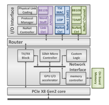
NaNet Architecture and Data Flow.
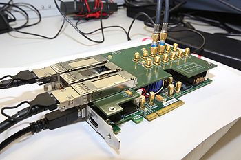
NaNet-1 implemented on an Altera Stratix IV coupled with a custom mezzanine card sporting 3 APE link channels.


NaNet-1
This version of the NIC features GPUDirect RDMA over 1 GbE and optionally 3 APElink channels. The design employs SGMII standard interface to connect the MAC to the PHY including Management Data I/O (MDIO); the MAC is a single module in FIFO mode for both the receive and the transmit sides (2048x32 bits). The logic resources consumption is shown in fig. (__)
Software Stack
Software components for NaNet-1 operation are needed both on the x86 host and on the Nios II FPGA-embedded μcontroller. On the x86 host, a GNU/Linux kernel driver and an application library are present. The application library provides an API mainly for open/close device operations, registration (i.e. allocation, pinning and returning of virtual addresses of buffers to the application) and deregistration of circular lists of persistent receiving buffers (CLOPs) in GPU and/or host memory and signalling of receive events on these registered buffers to the application (e.g. to invoke a GPU kernel to process data just received in GPU memory). On the μcontroller, a single process application is in charge of device configuration, generation of the destination virtual address inside the CLOP for incoming packets payload and virtual to physical memory address translation performed before the PCIe DMA transaction to the destination buffer takes place.
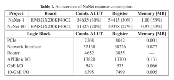
NaNet_1_10_Resource_Consumption.png.
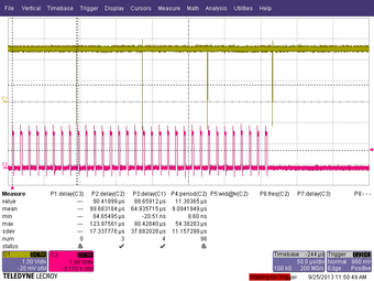
NaNet latency measurements performed with an oscilloscope.
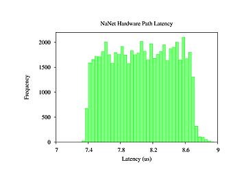
Distribution plot over 60000 samples of a NaNet trasversal time.


NIC packets traversal latency
In order to characterize the host+NIC system, a “system loopback” configuration was used: connecting one GbE interface of the hosting PC to the NaNet, it was possible able to generate and receive a UDP stream in a single host process, measuring latency as the difference of host processor Time Stamp Counter register at send and receive time of the same UDP packet (fig. __). Latency inside the NIC was measured adding 4 cycles counters at different stages of packet processing; their values are stored in a profiling packet footer with a resolution of 4 ns; for a standard 1472 bytes UDP packet, traversal time ranges between 7.3 us and 8.6 us from input of NaNet CTRL to the completion signal of the DMA transaction on the PCIe bus (fig. __). For the same packet size, saturation of the GbE channel is achieved, with 119.7 MB of sustained bandwidth. For scheduled improvements on the NaNet design see NaNet-10.
A physics case: the Level 0 trigger in NA62 Experiment's RICH Detector
NaNet is currently being used in a pilot project within the CERN NA62 experiment aiming at investigating GPUs usage in the central Level 0 trigger processor (L0TP) (ins. cit.). Data communication between the TEL62 readout boards and the L0 trigger processor (L0TP) happens over multiple GbE links using UDP streams. The main requisite for the communication system comes from the request for <1 ms and deterministic response latency of the L0TP: communication latency and its fluctuations are to be kept under control.
Performance Analysis
To carry on such measures, a "loopback" setup was used. That is, one of the host GbE ports had been sending UDP packets (according to the NA62 RICH readout data protocol) to the NaNet-1 GbE interface.
In this way, being the x86 TSC register a common reference time, it was possible in a single process test application to measure
- latency as time difference between when a received buffer is signalled to the application and the moment before the first UDP packet of a bunch (needed to fill the receive buffer) is sent through the host GbE port;
- time spent by GPU kernel on ring reconstruction.
Benchmarks results for GbE link and bandwidth/latencies