Difference between revisions of "ApeNEXT project"
From APEWiki
Jump to navigationJump to search| Line 15: | Line 15: | ||
* 6+1 on-chip, bidirectional, communication links with 200 MB/s of bandwitdh in LVDS technology. | * 6+1 on-chip, bidirectional, communication links with 200 MB/s of bandwitdh in LVDS technology. | ||
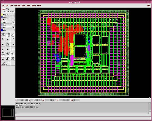
| − | [[Image:Apenext_jet_floorplan.jpg|right|500px| | + | [[Image:Apenext_jet_floorplan.jpg|right|500px|border]] |
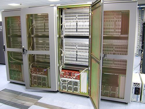
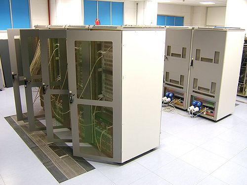
== apeNEXT computing center == | == apeNEXT computing center == | ||
Latest revision as of 11:14, 10 June 2011
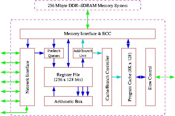
apeNEXT J&T processor design
The J&T processor has been designed in standard cell technology using the Atmel 0.18µ, 7 metal process. The chip die has a surface of 16x16 mm2 and contains 520K gates. The chip package is a BGA with 600pins. The chip target frequency is 200 MHz.
Processor highlights are:
- Low power consumption: 5W at 200MHz.
- Complex algebra is supported in HW, to accelerate LQCD computation.
- All data types have full 64 bit precision.
- A*B+C operator for all data types: integer, double, vector integer, vector double, complex.
- 8 KWord of on-chip instruction cache.
- 256 MB DDR DRAM plus error correction (EDAC).
- 128 bit, up to 200 MHz, local memory channel.
- 6+1 on-chip, bidirectional, communication links with 200 MB/s of bandwitdh in LVDS technology.


