APEmille project
A PARALLEL PROCESSOR IN THE TERAFLOPS RANGE
This document describes APEmille, a 3-D SIMD scalable parallel processor in the Teraflop range. This machine is very efficient for LGT simulations as well as for a broader class of numeric applications requiring massive intensive floating point computations.
Architectural Overview
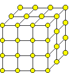
An APEmille machine can be viewed as a 3-D processing grid with periodic boundaries, composed of Processing Nodes. Each Processing Node is directly connected to its own 6 near-neighbours through synchronous data communication channels. The Processing Nodes are optimised for single precision floating point arithmetics and integer and double precision floating point operations are supported too. The SIMD paradigm (groups of nodes which execute the same instruction on different data) is complemented with a local addressing feature. Therefore all Processing Nodes may access their own local memories using different local addresses. This new feature is the most important extension to the present APE100 architecture, opening a path for coding of algorithms which could not be efficiently implemented on APE100 machines.
The local addressing capability is a valuable addition to the power, already present in the APE100 architecture, of the local conditional statements (Where(local condition)... Endwhere) and of global conditions derived by the set of local conditions (e.g. If(All(local condition)) ... Endif). A further enhancement to the APE100 architecture is represented by more general data routing capabilities among non-first-neighbour nodes.
While the computational kernel of APE100 is built using replicas of three kinds of boards (Controller Boards, Processing Boards and Communication Boards) an APEmille computational engine is based on multiple instances of just one Processing Board (PB). This design solution implies scalability and engineering advantages in comparison with the APE100 arrangement.
Each PB integrates all system functionality: flow control, data processing, internode communication and host<->APEmille I/O. A Root Board provides global synchronisation of the Processing Boards.
The host consists of one or more networked workstations, each controlling a group of PBs.
An APEmille machine can be partitioned into smaller SIMD machines, each comprising one or more Processing Boards, executing different instructions on each partition.
Each host in the network, using a high performance communication channel, maps the memories of a portion of APEmille (up to 128 nodes) on its own bus. The close integration with a network of host workstations allows a high input/output bandwidth with disks and peripherals in the range of 100 MByte per second per I/O device. Close integration of APEmille with standard workstation also adds the flexibility needed to customise the I/O system to the requirements of specific applications.
Topology
An APEmille machine is a 3D grid of processing nodes with hardware data links between the 3D first neighbouring nodes. The smallest machine is the single Processing Board (PB) where are placed 8 processing nodes with a 2x2x2 topology, (cube). Arranging togheter more PBs it's possible to have more complicated, greater and faster machines.
Hierarchical Hardware Topology
The yellow cubes in this rappresentation are single APEmille boards with their 8 processing nodes supposed as placed at the vertices of the cube.
- Board: 8 Nodes (2*2*2 topology)
- SubCrate: 4 Boards (2*2*8 topology)
- Crate: 4 SubCrates -16 Boards (2*8*8 topology)
- Tower: 4 Crates - 64 Boards (8*8*8)
- APEMille: 4 Towers - 256 Boards(32*8*8)
Performances
The following table reports the performance of the different configuration of an APEmille system: the maximum performance are about 1TeraFlops for the 66 MHz machine, and could be 1.6TFlops in a future 100 MHz release.
Comparing these performances, with an APE100 machine we find out that it's possible to replace an entire APE100 tower (25 GigaFloaps) with a APEmille SubCrate.
Processing node:
- 528 MegaFlops (66 MHz release)
- 800 MegaFlops (100 MHz release)
Board (8 nodes, 2*2*2):
- 4.2 GigaFlops (66 Mhz)
- 6.4 GigaFlops(100 Mhz)
SubCrate (4 Boards, 2*2*8):
- 16.8 GigaFlops (66 Mhz)
- 25.6 GigaFlops(100 Mhz)
Crate (16 Boards, 2*8*8, ~ 0.5 m^3):
- 66 GigaFlops (66 Mhz)
- 100 GigaFlops(100 Mhz)
Tower (4 Crates, 8*8*8, ~ 2 m^3):
- 264 GigaFlops (66 Mhz)
- 400 GigaFlops(100 Mhz)
APEMille (4 Towers, 32*8*8, ~ 8 m^3):
- 1 TeraFlops(66 Mhz)
- 1.6 TeraFlops(100Mhz)
Processing Board
Fore each APEmille PB a CPU takes care of the program flow and drives the communication protocol with the host network. The CPU broadcasts a VLIW (Very Long Instruction Word) to the 8 Processing Nodes located on each PB. At the same time, as a result of its calculations, the CPU broadcasts a Global Address to the Processing Nodes. The Nodes can access their own local memory using this Global Address either directly or after adding a local offset to it, thus producing a local address.
The 8 Processing Nodes of a Board are arranged in a cubic lattice (a 2x2x2 topology). Each processing node has an arithmetic and logic unit including floating point adders, multipliers, a large multiport register file plus a memory controller with address generation capability, interfacing to local memory. Integer and bitwise operations and local addressing are some of the new main features of the Processing Nodes.
The first APEmille systems, based on presently available Syncronous Dynamic Ram and VLSI ASIC technologies, will adopt a 66 MHz, 528 MFlops processor. We expect however that the clock frequency may eventually increase up to 100 MHz. A 2048 100 MHz nodes system would have a peak performance of 1.6 TeraFlops.
According to our application requirements, the size of the local memory of each Processing Node will range from 2 to 8 MWord. Through a Communication Device each Processing Node directly accesses the data on its own 6 neighbouring Nodes. Some routing capabilities allow of the comunication device (slower) access to far-away nodes.
The Processing Board hosts:
- 1 CPU
- 8 Processing Nodes,
- 1 Communication Device
- required memories.
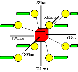
Scheme of connections among the 8 nodes of a PB
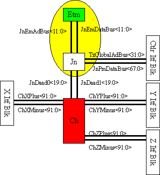
Cmille is the custom chip which takes care of the remote data communications between processing nodes.
Tmille is the custom processor which controls the instruction flow and global addressing of each APEMille SIMD partition (a minimum of 8 processing nodes). Tmille is connected to the Host, to its own data memory, to an instruction memory and to the Communication Device. It also drives the Address Bus. There is a major difference from the Ape100 machine where one controller CPU normally drives 128 nodes and is housed in a different board.
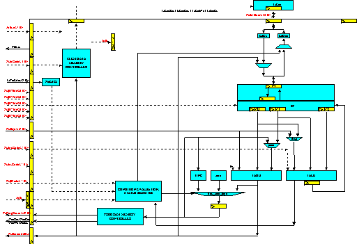
The Processing Node is composed of a floating point processor (called JMILLE) which drives its own Local Memory, receives Instructions and Global Addresses from TMILLE and communicates with the Communication Device (CMILLE).
The Communication Device also has a channel connected to the CPU, and through this pathway, to the Host. Through this pathway the Host loads the program and data memories of the floating point processor.
All the CPUs and all the Nodes of a SIMD machine partition execute the same instruction. Each PB sends its Local Signals to a Root Board and receives Global Signals from it, in order to manage Synchronisation, Exceptions and Global Flow Control Conditions.
Each Processing Board interfaces the Host through a dedicated synchronous channel (APE Channel) going from the CPU to the Host Interface.
Processing Node
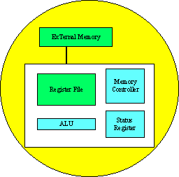
Each Processing Node is composed of a JMILLE floating point processor, attached to a SDRAM local memory. The Memory Controller inside Jmille generates addresses for the External Memory summing up a Global Address given by Tmille and a Local Address computed by Jmille itself. This way each APEMille Processing Node is able to generate a different Memory Address. The five addresses needed by the Multiport Register File are fixed by our compiler at compile time, and therefore distributed to Jmille inside the Program Word. This is obtained by means of our VLIW (Very Long Instruction Word) compiling technology.
Each Processing Node generates Status Signals (Global conditions, Exceptions etc.). These Status Signals are collected into a Global Status Return managed by the Control System. This connection allows the Control System to execute flow control instructions based on simultaneous logical conditions produced by the set of Processing Nodes. The instruction word read by JMILLE specifies the set of addressed location inside the large multiport Register File internal to JMILLE, and controls the Arithmetic Devices inside the processing node. Moreover it specifies Local Conditional Operation, Local Addressing functions, and Special Arithmetic function calculations to be performed by JMILLE.
Scheme of a Processing Node
- Jmille : is the APEMille custom arithmetic processor with hardware supporting arithmetic, logical and bitwise operations on complex, double precision, single precision and integer data types.
- External Memory (ETM) : A SDRAM memory, directly attached to Jmille and controlled by Jmille itself, where all the data related to the node processing are stored.
Tmille
Tmille is a VLSI device that includes all the control functions of the APEmille PB.
Tmille is composed of the following blocks:
- Decoder block: the interface to the host
- APEcontroller (ZCPU): controls the program flow (main sequencer, io_block, branch and address unit) and performs integer arithmetic and logical computations
- register block: status & exception registers
- Switch block: delivers data from the APE Channel to the proper PB device in download mode.
The host is able to access all the PB devices and memories through the APE Channel which is connected only to Tmille. Tmille is the APE Channel front end to the Processing Board. It decodes the APE Channel protocol and manages the data transfer between the APE Channel master (the host) and the requested APEmille device (memory or register). Tmille can assert the PB status according to the host requests and to the program requests. Two status are possible:
- system mode
- run mode.
In system mode the host can access all the PB memories and all Tmille, Jmille and Cmille registers. Tmille allows the host to download the executable file to the program memory and to download or upload data to/from its own data memory, the Jmilles's data memories and all the PB registers. The switch bus is used to send data from Tmille to the proper PB device.
In run mode the user program is actually running and the host cannot access neither the memories nor any Jmille or Cmille registers. Tmille waits over the APE Channel for a stop running request from the host.
The system_mode/run_mode switching must be performed accordingly to the Root Board directives to achieve the synchronisation of the Processing Boards. For this reason some signals ( halt, ifstatus .... ) must be delivered to the Root Board which collect them and send back the corresponding global signals to the PBs. (see PB Interconnections)
The APEcontroller takes care of the user program flow. In system mode the APEcontroller is idle. In run mode the APEcontroller runs the integer global part of the user program. The APEcontroller instruction is extended with the instruction to control the Jmille and Cmille units. Tmille, in run mode, halts the APEcontroller (switching into system mode) when the glb_halt flag is raised. Tmille in system mode starts the APEcontroller execution (switching into run mode) when the Root Board releases the glb_halt flag. The APEcontroller, in run mode, will conditionally branch on request testing the glb_ifstatus signal. Tmille raises the halt signal when the APEcontroller reaches a HALT instruction in the code or when an unmaskered exception occurs.
Tmille scheme
Control Word
Tmille is a VLIW processor. Its Control Word is 80 bits long and is composed of 10 fields as described in the following table.
| EDAC | IO | ALUFLOW | P4 | P3 | P2 | P1 | P0 | AGU | DISPL |
5 ALUFLOW ( Arithmetic Logic Unit)
2 AGU (Address Generation Unit)
3 IO (I/O code)
32 DISPL (address displacement)
6 RFP0 register file port 0
6 RFP1 register file port 1
6 RFP1 register file port 2
6 RFP1 register file port 3
6 RFP1 register file port 4
totale 72+8 EDAC = 80
Jmille
Cmille
PB interconnections
Each Processing Board has three different kinds of interconnections plus power supply and the global free-running clock:
- 3D data connections
- Global signals
- Root Board
- APE Channel
- The host PCI interface
- The Hippi Channel
- The Host Network
3D data connections
There are two bi-directional channels (one for each possible direction) in each of the three dimensions (X Y Z). Each channel is 80 bits wide and supports a transfer rate of 33-66 MHz (it is driven by the slow clock). Data transfers are point-to-point and EDAC corrected.
Global signals
The PB gives the following signals to the external world:
- ifstatus
- halt_requested
- CNB (Cmille Network Busy)
The PB receives the following signals from the Root Board and from the host:
- gbl_ifstatus
- gbl_halt
- gbl_CNB
- refresh
Root Board
The Root Board, the board which assures the global synchronisation of the Processing Boards - a critical feature of a SIMD machine, will receive local signals from the PBs and send back global signals to them as described in the previous section.
The signals glb_ifstatus, gbl_halt, and glb_CNB are set active if at least one of the corresponding local signals is active.The glb_clock_enable signal is always high unless one of the clock_stretch signals is active.The refresh signal is delivered to all the PBs according to the clock cycle and to the memory constraints.
APE Channel
Each PB is connected to the host network through the APE Channel. The APE channel is a 32 bits wide (+ EDAC), 33MHz, synchronous interface. All the PB's are slaves of the APE Channel. The APE Channel is in principle capable of a 133Mbyte/s performance (33MWords/s, 4 bytes each).Tmille interfaces the PB to the APE Channel. It waits for a valid control word on the APE channel. The control word contains the BoardId number to which the operation is requested, the operation code, the burst size and the direction of the transfer. When Tmille decodes an APE Channel control word it checks the BoardId in the control word against its own hard-wired SlotId or it checks if the control word is a broadcast request (directed to all the PBs). Shouldn't any of these situations occur, it ignores the control word and follows the transaction protocol without performing any PB operation. The second word in the protocol contains the address of the board device involved in the data transfer, while the data stream follows in the proper direction.
The host PCI interface
The APEmille Processing Boards will be interfaced with a network of computers equipped with Peripheral Computer Interconnect (PCI) I/O bus, which seems the emerging bus standard for workstations (133Mbyte/s). These computers will be referred to as APEmille Host Processors (AHP).
A Synchronous Interface will be implemented to connect the APE Channel to the PCI bus and a single AHP will be able to drive a set of Processing Boards (the ones connected to the same APE Channel; we call this set of boards an APEmille Unit: AU). The physical connection with the AHP is provided by a PCI interface board which will be plugged in one PCI slot in the AHP. Depending on the application requirements the number of PB driven by each AHP (i.e. the number of board in an AU) will be chosen to satisfy the needed I/O data rates. Up to 16 PBs can be connected to the same APE channel.The AHP will be able to access all the AU memories and control registers though the APE channel.
The Hippi Channel
The Host PCI Interface Board will host a driver for a HIPPI (High Performance Parallel Interface) channel.
Data coming from the APE Channel can be delivered either to the PCI host or to the HIPPI channel which can be connected to a high performance device such as a disk pack. The host drives the protocol initialisation with the PB and then switches the APE Channel path towards the HIPPI interface.Vice versa, the host can drive the PCI board so that after the protocol initialisation the boards can read data from the HIPPI channel.
This will allow very high data transfer performances. HIPPI is a mature communication technology with a rich I/O infra-structure developed for mainframes.
