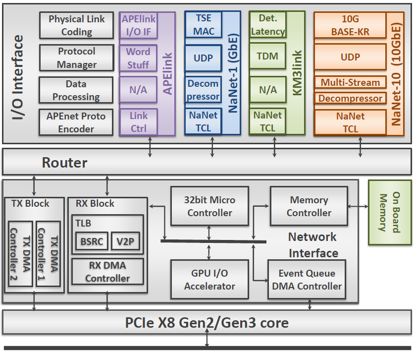
It performs a 4-stages processing on the data stream: following the OSI Model, the Physical Link Coding stage implements, as the name suggests, the channel physical layer (e.g. 1000BASE-T) while the Protocol Manager stage handles, depending on the kind of channel, data/network/transport layers (e.g. Time Division Multiplexing or UDP); the Data Processing stage implements application dependent transformations on data streams (e.g. performing compression/decompression) while the APEnet Protocol Encoder performs protocol adaptation, encapsulating inbound payload data in APElink packet protocol, used in the inner NaNet logic, and decapsulating outbound APElink packets before re-encapsulating their payload in output channel transport protocol (e.g. UDP).
It supports a configurable number of ports implementing a full crossbar switch responsible for data routing and dispatch. Number and bit-width of the switch ports and the routing algorithm can each be defined by the user to automatically achieve a desired configuration. The Router block dynamically interconnects the ports and comprises a fully connected switch, plus routing and arbitration blocks managing multiple data flows @2.8 GB/s
The block acts on the transmitting side by gathering data coming in from the PCIe port and forwarding them to the Router destination ports while on the receiving side it provides support for RDMA in communications involving both the host and the GPU (via the dedicated GPU I/O Accelerator module)
The module is built upon a powerful commercial core from PLDA that sports a simplified but efficient backend interface and multiple DMA engines.